In PCB and electronics manufacturing, relying solely on end-of-line inspection is a risky business. Hidden issues like cold solder joints or short circuits can bypass basic checks and trigger major product failures once deployed. For OEMs, that means costly replacements, warranty headaches, and damaged reputation
Last month, a client came to us after losing $25,800 in product returns—all due to severe BGA voiding and head-in-pillow (HiP) defects from their previous supplier. In high-density SMT assembly, over 70% of defects stem from solder paste printing errors and hidden solder joints that standard visual checks miss entirely.
At our EMS/PCBA facility, quality is not evaluated at the end; it is built into every step of the process. From raw Gerber files to the final working assembly, every board must clear 7 rigorous quality inspection gates before receiving shipping sign-off.
Step 1: Pre-Production Check — DFM & DFA Engineering Audit
Quality control doesn’t start on the factory floor—it starts with your files. Before we even cut a stencil or set up the SMT line, our engineers run your Gerber files, BOM, and assembly drawings through Valor DFM software, followed by a manual review..
We double-check for mismatched pads, layout risks, and component availability issues early on. Catching these tiny oversights on paper takes minutes; fixing them after production starts costs thousands. This simple check is how we keep your project on schedule and prevent costly scrap.
Step 2: Incoming Quality Inspection (IQC)
Garbage in, garbage out. A bad batch of ICs or a warped PCB will ruin the entire production run, no matter how good the SMT line is. That’s why every bare board and component is thoroughly inspected the moment it hits our warehouse.
What we verify before production starts:
- Bare PCBs: We check board thickness, copper weight, surface finish (ENIG, HASL, OSP), and panel warpage (kept under 0.75% so boards sit perfectly flat during assembly).
- Components: We test pin values with LCR meters, inspect leads for oxidation, verify Moisture Sensitivity Level (MSL) packaging, and screen for counterfeit or refurbished parts.
Step 3: Solder Paste Inspection (3D SPI)
Over 70% of SMT defects don’t happen during soldering—they happen way earlier, right at the solder paste printing stage. If the paste is too thick, too thin, or slightly offset, components will short or disconnect later.
To catch this immediately, our 3D SPI system scans 100% of the printed PCB pads in real time before a single component is placed.
What we check in real time:
- Paste Volume & Height: We measure the exact amount and thickness of solder paste on every single pad to prevent solder bridging or cold joints.
- Alignment & Bridge Risks: We inspect high-density footprints (like QFN, 0201, and 01005) to catch tiny alignment shifts and potential short circuits before boards head down the line.
Step 4: Automated Optical Inspection (AOI)
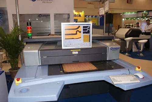
Human eyes get tired, but HD optical cameras don’t. To ensure every component sits exactly where it belongs, we run dual-stage AOI inspection both before and after reflow soldering.
How we inspect with dual-stage AOI
- Before Reflow (Pre-Reflow): We verify component presence, placement accuracy, and polarity (making sure diodes and capacitors aren’t flipped) before the board enters the oven, when corrections are still easy.
- After Reflow (Post-Reflow): Once soldered, high-speed HD cameras scan every joint for defects like tombstoning, solder bridges, lifted leads, and insufficient solder.
Step 5: 3D X-Ray Inspection for Hidden Joints
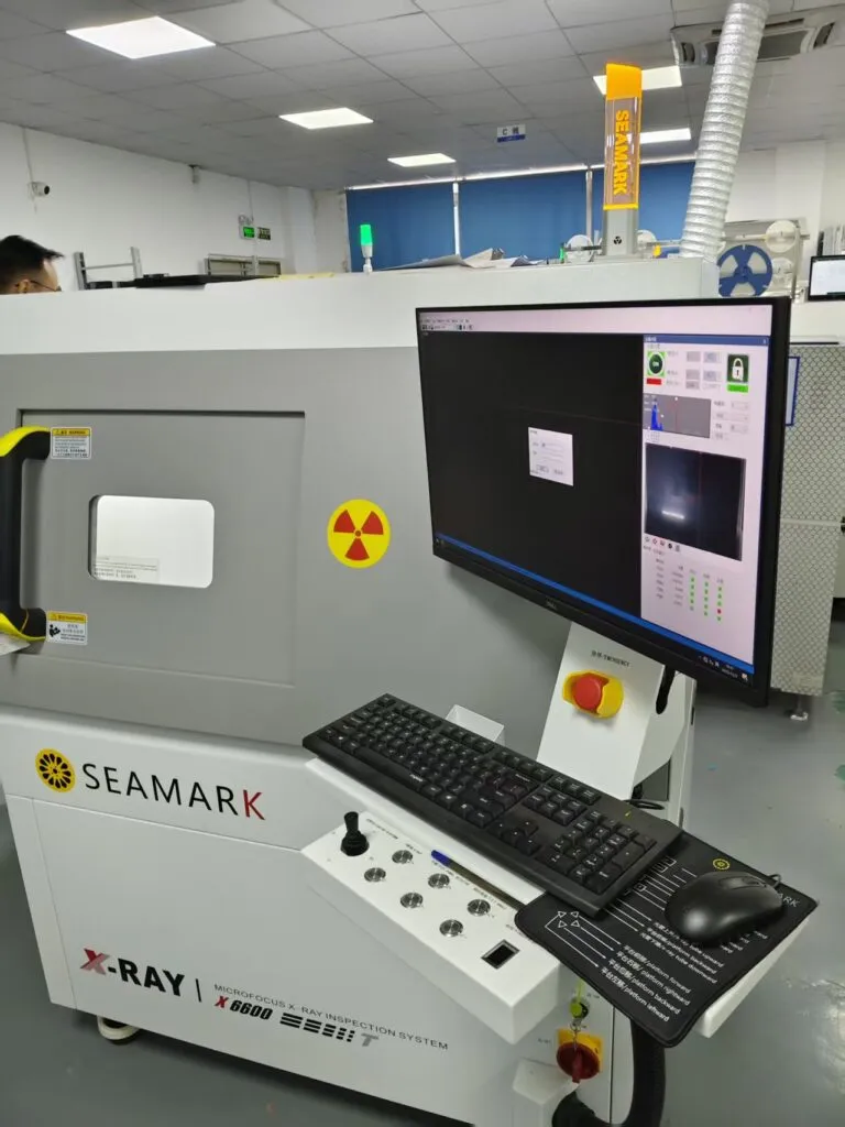
Modern chips like BGAs, QFNs, and CSPs hide their solder joints completely underneath the package—making them invisible to optical AOI cameras. Standard visual checks won’t spot a thing if a BGA ball fails to melt or bridges out of sight.tem
Our 3D X-Ray system sees right through the component body to inspect what’s happening underneath.
What we inspect under the chip:
- BGA Voiding: We measure air bubble percentages inside solder balls, keeping voiding strictly under 15% for standard boards and under 10% for high-reliability applications.
- Hidden Critical Defects: We scan for hidden solder bridges, ground pad voids, and Head-in-Pillow (HiP) defects where the solder touches but doesn’t fuse—preventing sudden product failures in the field.
Step 6: Through-Hole Assembly & Coating Quality
Not everything goes through SMT. For mixed-technology boards, through-hole (DIP) components still require precise wave soldering or manual insertion. To ensure stability, we lock down the process early by verifying the very first board (First Article Inspection) before running the whole batch.
What we check during final assembly:
- DIP Solder Joints: We check that the solder has properly filled the hole (at least 75% barrel fill) and that pins are trimmed to the correct length.
- Cleanliness & Coating: Leftover flux can cause short circuits later. We test the board for ionic contamination to make sure it’s completely clean, and use UV light to confirm that the conformal coating is applied evenly to protect against moisture and dust.
Step 7: Electrical and Functional Testing (ICT & FCT)
A board can look perfect under a camera, but the real question is: Does it actually work when you power it on? This final step ensures your PCBA functions flawlessly in the real world before we pack it for shipping.
How we verify performance:
- In-Circuit Testing (ICT): Using “bed-of-nails” fixtures, we test individual components (resistors, capacitors) and check for any hidden opens or shorts across the circuits.
- Functional Testing (FCT): We simulate your actual operating environment. We’ll power up the board, flash your firmware, test I/O ports, and verify wireless modules (Wi-Fi, Bluetooth) to guarantee it performs exactly as designed under load.
Quality Control Isn’t an Option—It’s Our Standard.
From Gerber analysis to final packaging, every board that leaves Jerico strictly meets IPC-A-610 Class 2 and Class 3 standards.
Planning a new board layout?
Send us your Gerber and BOM files today to request a Free DFM & DFA Review before committing to production. Our engineering team will help you spot hidden risks and optimize costs early on.