
Ask any hardware engineer about their favorite benchtop tool, and they’ll point to the digital multimeter. It’s the ultimate diagnostic gadget. You use it every day to check power rails, listen for that familiar continuity beep, and hunt down quick short circuits.
So, where’s the paradox? A multimeter is a savior on your workbench, but relying on it in mass manufacturing will wreck your business.
As modern circuit boards get denser and more complex—packed with tiny components, hidden solder joints, and ultra-thin traces—manual probing turns into a massive gamble.
Why Hand Probing Fails on the Factory Floor
While a multimeter is great for a quick health check, its physical design creates huge blind spots in high-volume production:
- No Physical Access: Modern microchips hide their tiny pins directly under the component body (like BGA or QFN packages). Your multimeter probes are simply too thick to reach underneath the chip to test those connections.
- Painfully Slow: Manually poking hundreds of tiny test points on a run of 1,000 boards takes hundreds of agonizing hours. It slows down delivery, creates huge bottlenecks, and practically guarantees human error.
- Invisible “Time-Bomb” Defects: A board might pass a simple multimeter beep today, but fail the moment a customer turns it on. A multimeter can’t measure solder volume, check if a joint will crack under heat, or tell you if a high-speed signal is degrading.
To guarantee near-100% yield, professional electronics manufacturers (EMS) completely ditch manual probing for large production runs. Instead, they implement multi-layered, automated quality control protocols that inspect, probe, and stress every board in a matter of seconds.
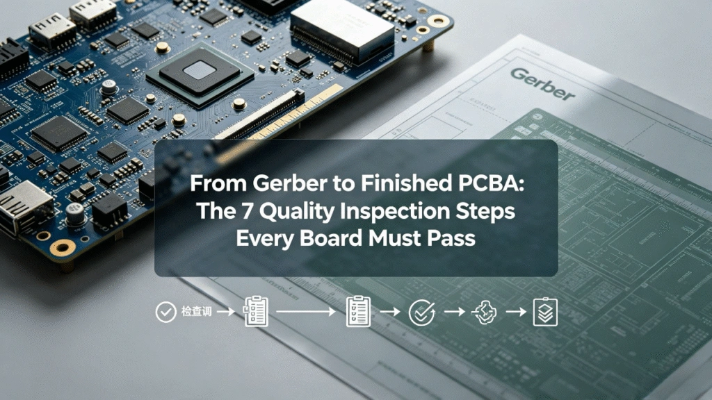
What is 7 Advanced PCB Testing Methods Used by Jerico
1. AOI (Automated Optical Inspection)
Inner & Outer Layer Fabrication
During inner and outer layer etching, high-resolution line-scan cameras photograph the copper pattern and compare every line and space directly against your original Gerber CAD files in real time. Catching a defect at this early stage is critical—once multi-layer boards go through lamination, an undetected inner-layer defect instantly turns an expensive raw panel into unrecoverable scrap.
Primary Focus: Micro-shorts, hairline opens, trace mousebites, pad pinholes, and copper line-width variations down to the micron level.
2. Microsection Analysis (Cross-Sectioning)
Post-Plating & Hole Wall Verification
While optical cameras inspect external features, destructive cross-sectioning is the only way to verify what is happening inside the copper barrel. We take sacrificial test coupons from the panel border, seal them in resin, grind them down, and inspect the internal structure under high-magnification metallographic optics to guarantee compliance with IPC-6012 Class 2 and Class 3 standards.
- Copper Plating Integrity: Measures precise electroplated copper thickness inside plated through-holes (PTH) and on outer surfaces.
- Structural Health: Detects resin recession, desmear efficiency, inner-layer interconnect failures, and thermal-stress issues like barrel cracking or delamination.
3. Electrical Testing (E-Test)
Bare Board Final Quality Control
No PCB leaves the fab house without 100% electrical continuity and isolation verification to guarantee zero open circuits or hidden shorts across all layers. Depending on your production scale and lead time, testing is routed through two distinct hardware setups:
| E-Test Method | Best Suited For | Operational Advantage |
| Flying Probe Testing | Prototypes & Quick-Turn | Zero fixture costs; ideal for fast turnarounds and smaller batch orders |
| Fixture Testing | High-Volume Mass Production | Tests hundreds of nets concurrently in seconds; drastically lowers unit testing cost |
4. Impedance Testing
Signal Integrity Check for High-Frequency Boards
For high-speed designs with controlled impedance rules, visual checks aren’t enough. We measure actual electrical signal reflection using Time Domain Reflectometry on integrated test coupons along the panel edge.
This ensures differential pairs, single-ended traces, and coplanar waveguides hit your exact target ohms (e.g., 50Ω or 100Ω differential) within strict tolerances (typically ±8% to ±10%).
5. Solderability Testing
Surface Finish Quality Control
To ensure the physical copper pads will accept customer solder seamlessly during assembly, sample boards undergo dip-and-look or wetting balance testing under accelerated aging conditions.
- Key Checks: Verifies the quality of surface finishes (HASL, ENIG, OSP, or Immersion Silver/Tin).
- Defects Prevented: Uncovers surface oxidation, finish degradation, or organic contamination before boards are shipped.
6. High-Pot & Thermal Shock Testing
Dielectric Breakdown & Reliability Verification
To guarantee long-term field reliability under harsh conditions, representative boards are subjected to high-voltage isolation (Hi-Pot) and rapid thermal cycling tests.
- Hi-Pot Test: Applies elevated voltage between isolated net pairs to ensure the FR-4 base material or prepreg layers do not experience dielectric breakdown.
- Thermal Shock: Exposes coupons to thermal cycling (e.g., solder float at 288℃) to stress the board, proving that micro-vias and multi-layer stackups won’t delaminate under customer soldering temperatures.
7. FQC & Final Visual Audit
Final Packaging & Outgoing Shipping Gate
The final line of defense combines automated visual inspection (AVI) with meticulous manual QA audits to inspect overall mechanical accuracy and cosmetics before vacuum sealing with desiccant:
- Dimensional Accuracy: Confirms total board thickness, outer routing tolerances, hole registration, countersinks, and V-scoring depth.
- Surface & Finish Quality: Audits ENIG gold thickness, solder mask coverage, silkscreen legibility, and gold finger beveling angles.
- Handling & Cleanliness: Guarantees zero ionic contamination, surface scratches, dust, or copper oxidation on exposed pads.
Our Jerico Quality Standard
Catching defects on a bare PCB requires layered line of defense—combining early optical scanning at the inner layers, rigorous physical cross-sectioning after plating, and 100% electrical validation before shipping.
By enforcing these seven inspection gates under IPC Class 2/3 standards, we ensure that every panel leaving our facility delivers structural integrity, predictable impedance, and flawless solderability for your downstream assembly.
Have specific DFM guidelines or stackup requirements for your next quick-turn or high-layer count build? Reach out to our Jerico engineering team for a full pre-production review.