Why does the cost of a multilayer PCB vary so much between different designs?
When engineers or procurement managers compare quotes for multilayer boards, they often find significant price gaps even for designs that appear similar on the surface. The reality is that multilayer PCB pricing is never determined by layer count alone.
The cost of multilayer PCB manufacturing depends on more than the number of layers. PCB stackup, copper thickness, material selection, impedance requirements, board size and production volume can all affect the final cost.
Understanding how these engineering decisions impact multilayer PCB manufacturing allows teams to optimize their designs for both performance and yield without paying for unneeded manufacturing complexity.
What is a Multilayer PCB?
A multilayer PCB is a printed circuit board containing three or more conductive copper layers separated by insulating dielectric materials (cores and prepregs) and bonded together under high heat and pressure.
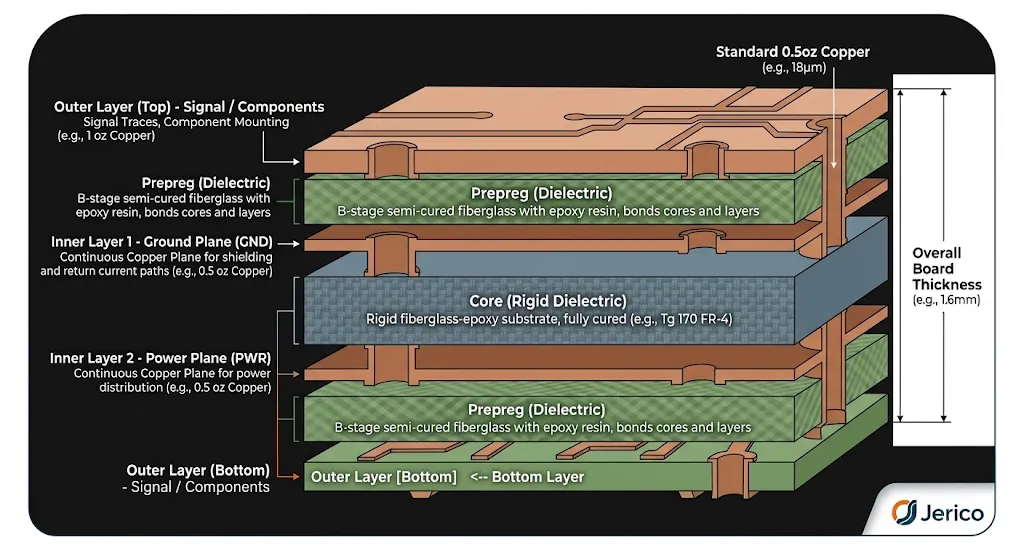
While 2-layer boards remain common for simple power supplies or basic controls, modern electronics increasingly demand 4-layer, 6-layer, 8-layer, 10-layer, 12-layer, and high-layer-count PCBs (stretching to 32+ layers).
How Does Layer Count Affect Multilayer PCB Cost?
Layer count is the most obvious cost driver, but its financial impact is non-linear. Moving from 4 layers to 6 layers does not simply add 50% to the bill; it introduces additional material sheets, inner-layer imaging steps, AOI (Automated Optical Inspection), and extra lamination cycles.
| Layer Count | Typical Applications | Cost Impact |
| 4 Layer | Industrial controls, consumer electronics, simple IoT | Lower (Base multilayer standard) |
| 6 Layer | Automotive modules, networking devices, embedded systems | Moderate (~30%–40% over 4-layer) |
| 8 Layer | High-density processing boards, medical instrumentation | Higher (Requires tighter registration) |
| 10-12 Layer | High-speed routers, complex server hardware, aerospace | Higher (Requires precise material stability) |
| 14+ Layer | Supercomputing, advanced defense systems, backplanes | Project-Dependent (Yield-sensitive) |
Note: Exact pricing depends on panel efficiency, material choice, and fabrication tolerances.
The Hidden Cost Drivers of High Layer Counts
- Lamination Cycles: Higher layer counts require precise registration during the multi-layer bonding process. Misalignment causes inner-layer shorts or broken via connections.
- Drilling Complexity: Deeper drill holes mean lower aspect ratios (Ratio of board thickness to hole diameter). High aspect ratios require slower drill speeds and specialized plating processes to ensure copper covers the entire barrel wall uniformly.
Why PCB Stackup Matters
A board’s PCB stackup defines its physical architecture: the exact arrangement of conductive signal layers, solid power planes, continuous ground planes, dielectric core thicknesses, and prepreg types.
An unoptimized stackup directly increases manufacturing costs and leads to field failures:
- Symmetry and Warpage: Stackups must be balanced around the center axis. Asymmetrical dielectric thicknesses or uneven copper distribution cause the board to twist or bow during reflow soldering.
- Standard Stock Materials vs. Custom Dielectrics: Specifying non-standard prepreg glass styles or rare core thicknesses forces manufacturers to make special material purchases, adding lead time and minimum order quantity (MOQ) surcharges.
- An engineered stackup balances mechanical stability, target board thickness (e.g., 1.6mm), signal integrity, and manufacturing yield.
How Copper Thickness Affects Cost
Standard multilayer boards typically use 0.5 oz or 1 oz copper for inner layers and finished 1 oz copper for outer layers. Increasing copper thickness directly impacts fabrication complexity.
The Cost Implications of Thicker Copper
- Etching Overhead: Thicker copper requires longer etching cycles, which creates “etch factor” challenges (undercutting). Manufacturers must adjust trace widths during CAM preparation to compensate.
- Resin Infill: Heavy copper layers leave larger gaps between traces. To prevent air bubbles (voids) during lamination, thicker or higher-resin prepregs must be used to encapsulate the copper completely.
- Trace/Space Limitations: Heavy copper cannot support ultra-fine pitch traces. A 3oz copper layer typically requires minimum trace widths and spacing of 8/8 mil or higher.
For high-current applications, heavy copper PCB may be more appropriate than standard multilayer PCB designs.
How Impedance Control Affects Multilayer PCB Manufacturing
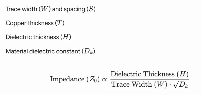
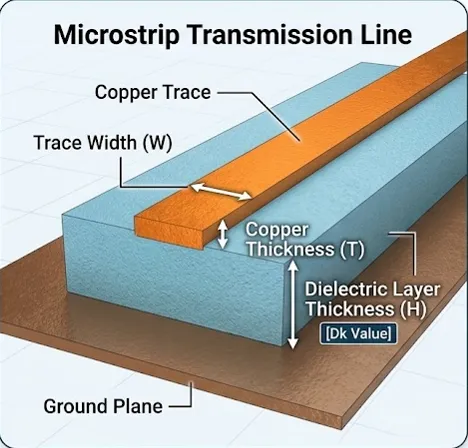
High-speed digital interfaces (PCIe, USB 3.2, Ethernet, DDR memory) demand controlled impedance to prevent signal reflections and data loss. Target impedance (e.g., 50Ω single-ended, 90Ω or 100Ω differential) depends on:
Why Impedance Control Adds Manufacturing Cost
- Tight Process Tolerances: Maintaining ± 10% (or ±5%) impedance tolerances requires strict control over etching line widths and dielectric thickness consistency.
- Coupon Testing & Quality Control: Every production panel must include dedicated test coupons. Fabricators verify impedance using Time Domain Reflectometry (TDR) test equipment and generate compliance reports prior to shipment.
- Panel Utilization: Test coupons take up space on the manufacturing panel, slightly reducing overall panel efficiency.
Pro Principle: Impedance requirements should be considered during initial stackup design rather than treated as a final-stage inspection item. Consulting your manufacturer early prevents redesigns caused by unavailable core thicknesses.
Other Factors That Affect Multilayer PCB Cost
Beyond layer count, stackup, copper weight, and impedance, several manufacturing variables influence total unit cost:
- Substrate Material: Standard FR-4 (Tg 135) is economical. High-Tg FR-4 (Tg 170+), halogen-free materials, or high-speed low-loss laminates (e.g., Megtron 6, Rogers) carry higher raw material costs.
- Via Technology: Standard through-hole vias are the most economical. Adding blind vias, buried vias, or microvias (HDI technology) requires sequential lamination steps and laser drilling, increasing costs.
- Surface Finish: Lead-Free HASL is cost-effective. ENIG (Electroless Nickel Immersion Gold), ENEPIG, or Hard Gold add plating costs but offer flat surfaces for fine-pitch BGAs.
- Board Dimensions & Panelization: Odd-shaped boards or unoptimized panel dimensions increase material waste.
- Production Volume & Testing: Prototype runs incur setup fees spread across a few units. Production volumes amortize setup costs, significantly lowering price per unit.
Multilayer PCB Manufacturing Process
Understanding the production workflow clarifies why precise manufacturing capabilities matter for high-reliability boards:
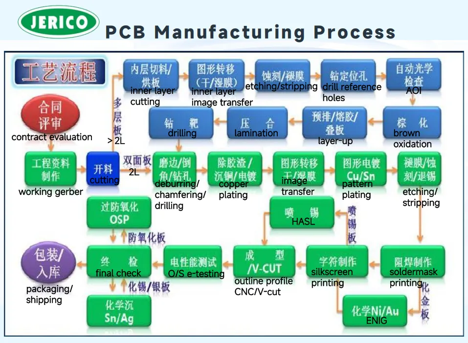
How to Choose a Multilayer PCB Manufacturer in China
Selecting the right manufacturing partner ensures high yield, signal integrity, and long-term product reliability. When evaluating offshore or China-based PCB fabricators, assess the following critical capabilities:
- Layer & Structural Capability: Can the fabricator produce high-layer-count boards (12–32+ layers) with precise layer registration?
- Stackup Engineering Support: Do they provide pre-layout stackup calculations and material suggestions?
- Impedance Control Assurance: Do they provide 100% TDR coupon test reports with shipped orders?
- Advanced Via & Material Options: Do they support HDI, microvias, heavy copper, and hybrid material stackups?
- Quality Management System: Are they certified to IPC Class 2/Class 3, ISO 9001, and IATF 16949 standards?
- Clear Engineering Communication: Can their CAM team quickly review Gerber/ODB++ files, resolve DFM issues, and confirm specs before production starts?
Partnering with Jerico PCB
Jerico supports multilayer PCB production from rapid prototypes to high-volume manufacturing, offering capabilities up to 32 layers, precise controlled impedance tolerances, complex stackup engineering, and comprehensive DFM reviews before fabrication.
Need a Multilayer PCB for Your Next Project?
Share your Gerber files, stackup requirements, and project specifications with our engineering team for a comprehensive DFM review and instant quote.