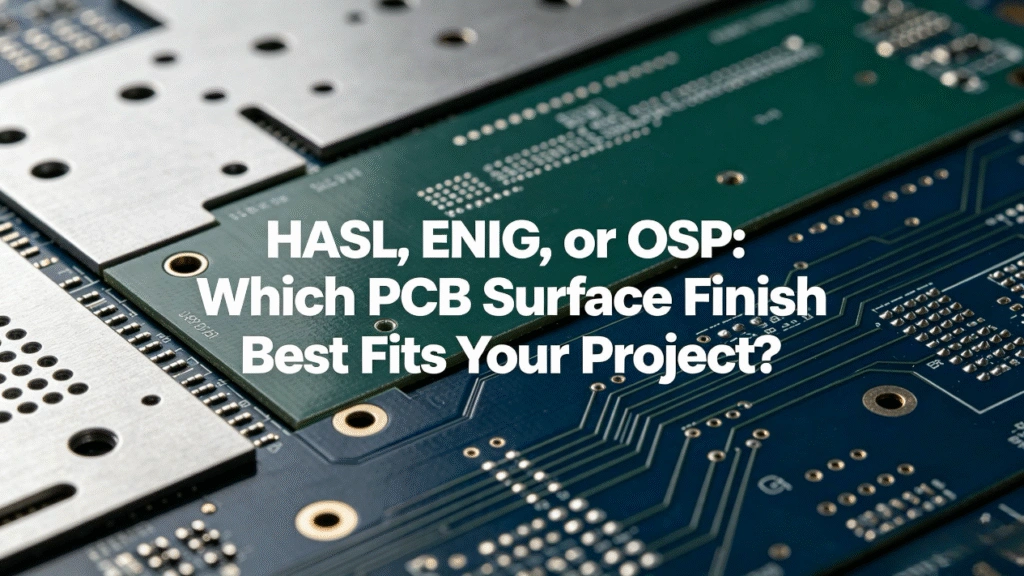
Choosing the right PCB surface finish is one of the most critical decisions in the printed circuit board manufacturing process. The surface finish protects the exposed copper traces from oxidation and creates a solderable surface for component assembly.
However, with multiple options available, each offering distinct advantages in terms of cost, shelf life, and assembly compatibility, making the right choice can be challenging.
In this guide, we break down three of the most popular PCB surface finishes—HASL (Hot Air Solder Leveling), ENIG (Electroless Nickel Immersion Gold), and OSP (Organic Solderability Preservatives)—and provide a clear comparison to help you choose the best option for your project.
1. Quick Comparison Table
To give you an immediate overview, here is how HASL, ENIG, and OSP compare across key engineering and purchasing parameters:
| Parameter | HASL (Leaded / Lead-Free) | ENIG | OSP |
| Relative Cost | Low | High | Very Low |
| Shelf Life | Long (12+ Months) | Very Long (12+ Months) | Short (6 Months) |
| Surface Flatness | Poor (Uneven) | Excellent | Excellent |
| Solderability | Excellent | Excellent | Good |
| Fine-Pitch / BGA | Not Recommended | Excellent | Good |
| Thermal Cycles | Moderate | Excellent | Moderate |
| RoHS Compliance | Leaded: No / Lead-Free: Yes | Yes | Yes |
2. In-Depth Overview of Each Finish
2.1 HASL (Hot Air Solder Leveling)
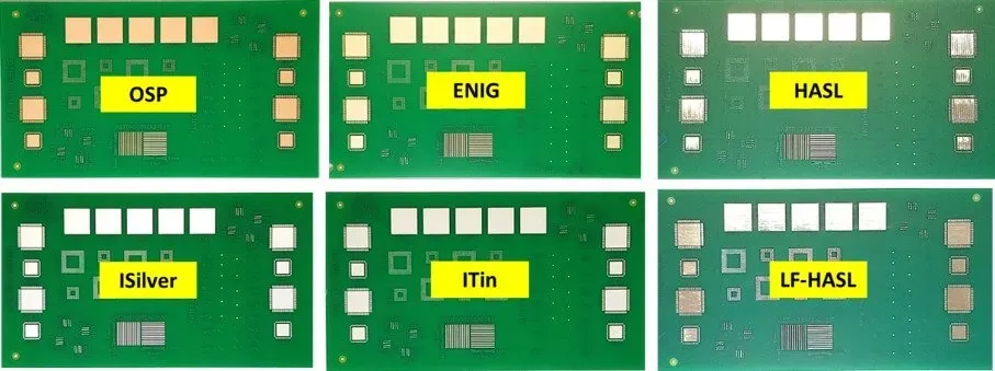
HASL is the traditional workhorse of the PCB industry. The board is submerged in molten solder, and hot-air knives blow off the excess solder to level the surface.
Pros: Highly cost-effective, robust solder joint reliability, easily reworkable, long shelf life.
Cons: Non-flat surface. The thick solder bumps make it unsuitable for high-density components like Fine-Pitch SMT or BGAs (Ball Grid Arrays).
Best For: Standard through-hole boards, low-density SMT designs, and budget-sensitive projects where flat surface coplanarity isn’t strict.
2.2 ENIG (Electroless Nickel Immersion Gold)
ENIG is a two-layer metallic coating consisting of a nickel layer topped with a thin layer of immersion gold. The nickel acts as a barrier to the copper and the surface to which the components are soldered, while the gold protects the nickel during storage.
Pros: Extremely flat surface (ideal for fine-pitch BGA and small SMT components), excellent corrosion resistance, long shelf life, and good for aluminum wire bonding.
Cons: Higher cost compared to HASL and OSP. Requires careful manufacturing process control to prevent “black pad” issues.
Best For: High-density PCBs, complex multi-layer boards, medical, automotive, or industrial electronics requiring maximum reliability.
2.3 OSP (Organic Solderability Preservatives)
OSP applies a water-based, ultra-thin organic layer over the exposed copper. This layer selectively binds to copper and provides an organometallic layer that protects the copper prior to soldering.
Pros: Low cost, simple manufacturing process, environmentally friendly (RoHS compliant), and provides a very flat surface for SMT assembly.
Cons: Short shelf life (requires assembly within 6 months), sensitive to handling (touching with bare fingers damages the protective film), and limited reflow cycles.
Best For: High-volume consumer electronics, flat SMT layouts with tight budgets, and projects with quick production turnaround.
3. How to Choose for Your Next Project?
When deciding between HASL, ENIG, and OSP, consider these three core factors:
1. Component Pitch & Density: If your design features fine-pitch components (0.4mm pitch or smaller) or BGAs, choose ENIG or OSP for their flat surfaces. Avoid HASL.
2. Budget vs. Performance: For maximum cost efficiency in high-volume production, OSP is ideal. For budget projects with simple component density, HASL works best. For premium reliability and performance, invest in ENIG.
3. Storage & Handling: If your boards might sit in inventory for over 6 months before assembly, ENIG or HASL are far safer choices than OSP.
4. Get Expert DFM & Surface Finish Guidance
At Jerico PCB, we bring over 17 years of experience in high-reliability PCB manufacturing and assembly. Our engineering team conducts free DFM (Design for Manufacturability) checks on every project to ensure your selected surface finish perfectly balances performance and cost.
Have questions about your PCB design? [Request an Online Quote] or send your Gerber files to sales16@pcbjust.com for a free quotation and technical review!