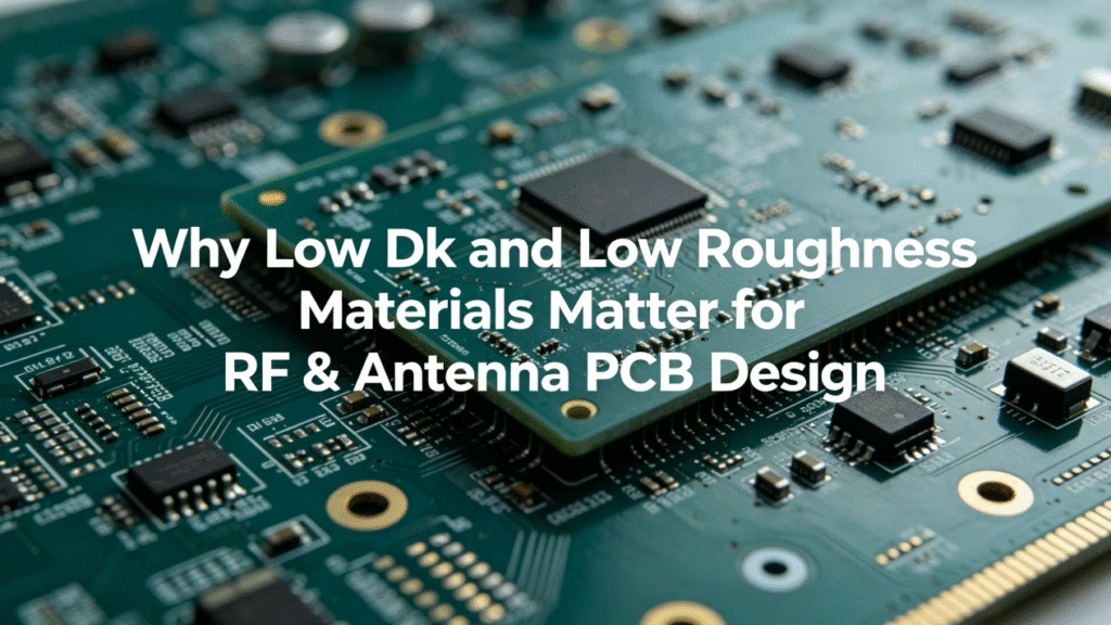

Multilayer PCBs are the backbone of modern high-performance electronics. As designs demand higher routing density, stable power delivery, controlled impedance and reliable thermal management, simple 2-layer boards often reach their limits. This guide walks hardware engineers and procurement buyers through multilayer PCB fundamentals, board variants, fabrication workflow, stack-up considerations and supplier selection criteria. You will also find key checkpoints to prepare accurate RFQs and prototype orders.
1. What Is a Multilayer PCB?
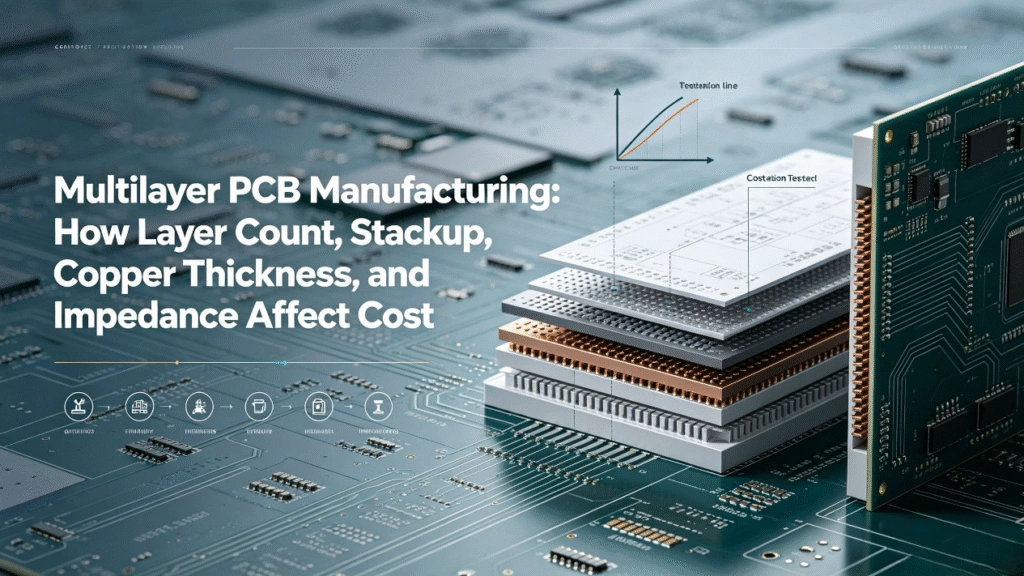
A multilayer PCB is constructed with three or more copper conductive layers, bonded together using dielectric prepreg insulation. Electrical connections between separate copper layers are achieved via plated through-holes, blind vias or buried vias.
Unlike double-sided PCBs that only have copper on the top and bottom surfaces, multilayer designs can dedicate entire inner layers for ground planes, power planes or sensitive signal traces. This architecture solves common design challenges including EMI noise, poor power integrity and routing congestion.
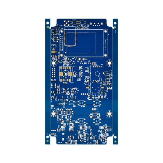
6-layer FR-4 multilayer PCB (PCB-54) with ENIG finish, 0.15 mm minimum hole size and 3 mil minimum line spacing.
2. When Do You Need to Upgrade From Double-Sided PCB?
A double-sided PCB provides two conductive layers, one on each face of the substrate. That is sufficient for simple circuits, but signal routing, power delivery and ground return all compete for the same two surfaces as soon as a design grows. The result is usually visible: wider boards, more routing compromises, uncertain return paths for high-speed signals, and electromagnetic interference that is hard to contain.
Multilayer construction solves this by dedicating whole layers to a single job. A four-layer board typically assigns two layers to signal routing and two to power and ground. A six-layer board adds further separation, so sensitive signal layers can sit next to a solid reference plane instead of sharing space with switching currents.
Benefits of adding extra layers
- Routing capacity: more channels per square millimetre of board area, so the package footprint can shrink.
- Power integrity: a dedicated power plane and ground plane lower loop inductance compared with thin traces on a two-layer board.
- Controlled impedance: signal layers adjacent to a continuous reference plane make a defined trace geometry reproducible, which is what impedance control depends on.
- Shielding and EMI behaviour: internal planes act as a barrier between noisy and sensitive nets.
- Thermal spreading: internal copper distributes heat away from power devices.
Cost impact of extra layers
- Multilayer production relies on repeated lamination, not simple printing.
- Each extra layer pair needs inner layer imaging, etching, oxide treatment, layup and lamination. More lamination cycles bring higher risks of registration deviation, resin flow variation and board warpage.
- Qualified multilayer factories are equipped with LDI direct imaging, vacuum lamination, AOI, X-ray inspection and metallographic cross-section analysis. These process controls are essential and should be confirmed during quotation.
3. PCB Market & Industry Standards
Multilayer PCB is mainstream in the PCB industry, not a niche product. Prismark data: global bare PCB market reached USD 85.8B in 2025, estimated USD 95.8B in 2026. Multilayer PCB takes around 52% of total production volume. China will contribute roughly 60% of global PCB output in 2026.
For buyers:
- Multilayer capacity is easy to source. Select suppliers based on technical capability, document support and process control, not just availability.
- The gap between different suppliers lies in tolerance control, raw material management and quality evidence.
Common IPC standards you will see in purchase documents:
- IPC-A-600: PCB acceptance criteria
- IPC-6011 / IPC-6012 / IPC-6013: Specification for generic, rigid and flexible PCB
- IPC-4101F: Material standard for rigid & multilayer PCB
- IPC-4204C: Material standard for flexible metal-clad dielectric
4. Main Types of Multilayer PCB
“Multilayer” describes the stacking structure, not one single product. Below are common types and typical application scenarios:
Made of rigid substrate (mostly FR-4), keeps shape after assembly. Jerico supplies rigid PCB from 1–18 layers, including popular 4-layer and 6-layer versions for consumer, industrial and automotive electronics.
2. Double-Sided PCB
2-layer rigid PCB. Low cost for simple circuits, your baseline reference to judge whether multilayer is necessary.
3. HDI Multilayer PCB
HDI uses laser microvias, blind & buried vias and sequential lamination to achieve ultra-high routing density that normal through-hole multilayer cannot reach. Jerico HDI examples:
- TU-883: 18-layer 2-step HDI, stack-up 2+14+2
- M7: 32-layer 3-step HDI, stack-up 4+24+4 Suitable for HPC, telecom, automotive, medical and military electronics.
4. Heavy Copper Multilayer PCB
Thick copper plating for high current carrying and heat dissipation, widely used in power circuits.
5. Metal Core / Aluminum Base PCB
Metal substrate for fast heat dissipation. Mainly for LED and power modules, usually single-sided or simple multilayer.
6. High Frequency / Rogers PCB
Low-loss laminate instead of standard FR-4 to keep stable signal performance at high frequency. Rogers is a laminate brand, not a PCB type. You need to confirm dielectric parameter and loss data at RFQ stage.
7. Flex, Rigid-Flex, Ceramic & Cavity PCB
- Flex PCB: polyimide base, bendable
- Rigid-Flex PCB: combine rigid section and flexible section
- Ceramic PCB: excellent thermal conductivity and thermal stability
- Cavity PCB: recessed pocket inside stack-up to reduce overall component height
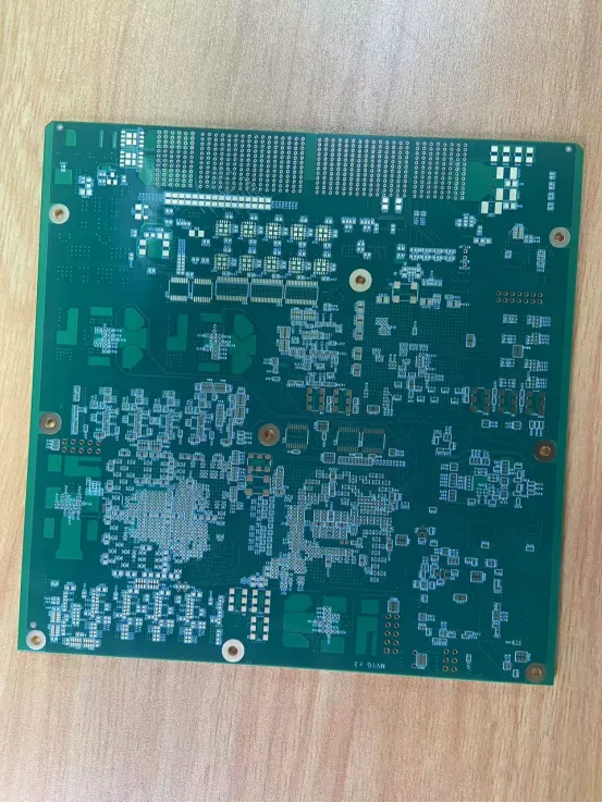
TU-883 hsd hdi 18L — 18-layer, 2-step HDI multilayer PCB with a 2+14+2 stack-up and 0.5 mm minimum BGA pitch
5. Multilayer PCB Manufacturing Process Step by Step
Multilayer boards are built from inner core pieces, processed and laminated together. Below is standard production flow with quality check points:
- DFM & Data Review: Check Gerber, stack-up, impedance requirement, drill file and panel design before production
- Inner Layer Imaging: Dry film exposure; LDI direct imaging for fine trace production
- Inner Layer Etching & AOI Inspection: Remove unwanted copper; AOI catches open/short before lamination
- Oxide Treatment & Layup: Copper surface treatment for adhesion; stack cores and prepreg as required
- Vacuum Lamination: Bond all layers under heat & pressure; high Tg material (Tg170 / Tg180) used to avoid warpage after multiple reflow
- Drilling: Mechanical drill for through holes; laser drill for HDI microvias
- Copper Plating & Outer Layer Imaging: Plate copper on hole wall and surface, then pattern outer layers
- Solder Mask & Silkscreen Printing: Custom mask color and legend
- Surface Finish: ENIG / ENEPIG / OSP / HASL etc. ENIG is preferred for fine pitch BGA and anti-oxidation
- Electrical Test & Inspection: Flying probe test for small batch, fixture E-test for mass production; AOI, X-ray and cross-section check for hidden defects
- Final Inspection & Packing: Final FQC, vacuum packing for shipment
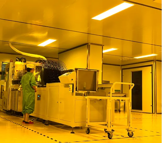
Film handling in a Class 10,000 clean room — one of the process environments behind fine-line multilayer imaging
6. Key Stack-Up Parameters That Affect Cost & Yield
Most cost and yield risk are determined at the design stage by stack-up specification. Focus on these items:
- Layer count & stack symmetry: Asymmetric stack brings stress and warpage risk
- Base material & Tg: Standard FR-4 for consumer; high Tg FR-4 for automotive and thermal cycling environment
- Copper weight: 1oz common for signal; 2oz for high current and heat dissipation
- Min line width & space: Determines routing density. Jerico mass production capability: 3/2.8 mil, impedance tolerance ±10%
- Min hole size: 0.2 mm for 4-layer; 0.15 mm for 6-layer; smaller holes need HDI process
- Surface finish selection: HASL/ ENIG/ ENEPIG
- Board thickness & tolerance: 1.0/1.2/1.6 mm standard; HDI up to 2.4mm / 3.2mm
- Inspection class: IPC Class 2 (general electronics), IPC Class 3 (high reliability)
- Test method: Flying probe for prototype / low volume; fixture test for mass production
Product Spec Comparison Table
| Model | Type and layers | Base material | Surface finish | Min. hole | Min. line / space | Copper | Board thickness | MOQ |
| PCB-10 | Rigid 4L | FR-4 | Lead-free HASL | 0.2 mm | 3 mil | 1 oz | 1.0/1.2/1.6mm / custom | 1 pc |
| PCB-54 | Rigid 6L | FR-4 | ENIG | 0.15 mm | 3 mil | 2 oz finished | 1.6 mm | 1 pc |
| PCB-55 | Rigid 6L | FR-4 | ENIG | 0.15 mm | 3 mil | 1 oz | 1.6 mm | 1 pc |
| PCB-56 | Rigid 4L | FR-4 | ENIG | 0.15 mm | 3 mil | 1 oz | 1.0 mm | 1 pc |
| PCBA-999 | 4L PCBA | FR-4 | Lead-free HASL | 0.2 mm | 3 mil | 1 oz | 1.2 mm | 1 pc |
| TU-883 hsd hdi 18L | 2-step HDI, 18 layers,2+14+2 | High Tg FR-4 ≥170℃ | ≥170℃ ENIG + hard gold on finger |
— | — | 2oz inner & outer | 2.4±0.10 mm | — |
| M7 | 3-step HDI, 32 layers, 4+24+4 | High Tg FR-4 ≥180℃ | ENIG + hard gold on finger | — | — | 2oz inner & outer | 3.2±0.10 mm | — |
HDI extra specs:
TU-883: Min BGA pitch 0.5mm; M7: Min BGA pitch 0.4mm
Both support differential 100Ω ±8%, single-ended 50Ω ±10% for PCIe high-speed signal, IPC 6012 Class3, UL94 V-0
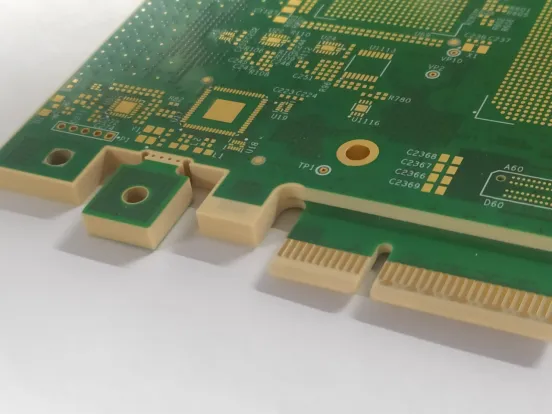
M7 — 32-layer, 3-step HDI multilayer PCB with a 4+24+4 stack-up, 0.4 mm minimum BGA pitch and 0.8 mm step depth
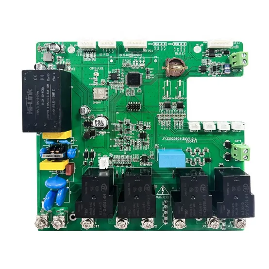
PCBA-999 — 4-layer FR-4 multilayer board supplied with SMD, SMT and DIP assembly as a single turnkey build
7. Application Fields of Multilayer PCB
1. Automotive Electronics
Work temperature: -40℃ ~ +125℃, service life 10–15 years, resistant to salt spray, moisture and EMI. Spec preference: High Tg FR-4, CAF resistance, UL94 V0, ENIG, IPC Class3. Mass automotive orders need PPAP, material certificates, impedance report and batch traceability.
2. Telecom & Networking
For router, switch, high-speed BGA fanout, stable controlled impedance. HDI with resin-filled microvia and via-in-pad is widely used.
3. Industrial, Security & Medical Device
Prioritize long service life, stable supply and change control. 4/6 layer rigid PCB is mainstream.
4. Consumer 3C, IoT & Smart Home
Cost-sensitive, compact size. Lead-free HASL + panel design with stamp holes for easy depaneling.
5. PCB Prototype & Low Volume Custom Service
Support 1pcs prototype validation, vacuum packing. Turnkey PCBA service available (PCBA-999: SMT + DIP assembly).
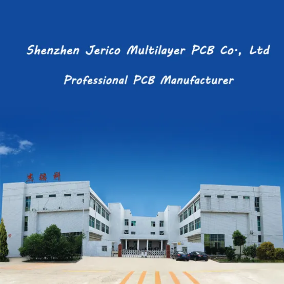
Jerico’s manufacturing base in Wuping, Fujian — a 20,000 m² facility with monthly capacity of 50,000 to 70,000 m²
8. How to Select a Qualified Multilayer PCB Supplier
Because multilayer capability is widely available, the useful screening question is not “can this supplier make a multilayer board” but “can this supplier prove what it made”. A workable checklist for the research stage:
- Clear capacity range: max layer count, HDI process, special material capability
- Valid certificates: UL file number, IATF16949, ISO9001, ISO14001, RoHS & REACH report
- Testing equipment: LDI, vacuum lamination, AOI, X-ray, flying probe, reliability lab (salt spray, cross section)
- Document support: impedance report, material COC, test report, PPAP for automotive
- Batch traceability and corrective action process
- Export experience, familiar with overseas packing & document requirement
9. About Jerico PCB
SHENZHEN JERICO MULTILAYER PCB CO., LTD (JRC / JERICO) is a PCB fabrication and partial PCB assembly supplier based in Shenzhen, Guangdong, China. The company was established in 2009 and reports more than 15 years of PCB manufacturing experience, operating two bases: a manufacturing site in Wuping, Fujian, and a business centre in Shenzhen, Guangdong.
- Team: ~270 people, 30 R&D engineers
- Monthly capacity: 50,000 ~70,000 m²
- Export ratio: 40% of sales, main market EU & USA
- Key customers: Xiaomi, ZTE, Ecovacs, BDstar, Changhong, Legrand
- Product range: Rigid PCB 1–18L, heavy copper, HDI, high frequency, metal core PCB
- Process capability: 3/2.8 mil min line/space, impedance ±10%
- Quality system: IPC-A-600H, IPC-6012, UL796, IATF16949
- Service: 7×24 technical support; complaint response within 24h, CAPA report within 72h
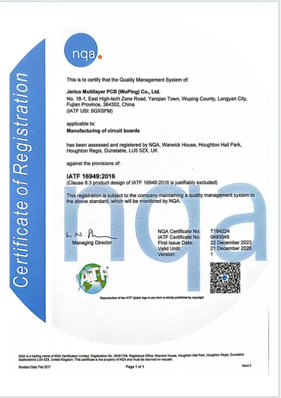
IATF 16949:2016 automotive quality management system documentation — relevant when multilayer boards enter automotive supply chains
10. FAQ
Q1: What standards and certificates should I check?
A: Acceptance standard IPC-A-600; performance IPC-6011/6012/6013; material IPC-4101F / IPC-4204C.
Supplier certificates: ISO9001, ISO14001, IATF16949 (automotive), UL, RoHS, REACH SGS. Confirm certificate scope and revision.
Q2: What multilayer complexity can Jerico support?
A: Rigid PCB up to 18L, heavy copper, HDI blind/buried via, high frequency, metal core PCB.
HDI flagship: 18L 2-step HDI and 32L 3-step HDI for high-speed PCIe, Class3 reliability.
Q3: What files & info do I need for accurate quotation?
A: Gerber, stack-up, material & Tg, copper weight, board dimension & thickness, min line/hole, surface finish, solder mask color, quantity, test method.
If PCBA needed, provide BOM and assembly requirement.
Q4: Can I order only 1 piece for prototype test?
A: Yes. 4L and 6L PCB support MOQ 1pcs, vacuum packing, flying probe test available.
Q5: What is the lead time difference between prototype and mass production?
A: Lead time depends on layer count, material and surface finish. HDI 18L/32L needs multiple lamination cycles and longer time. Send your stack-up and quantity for exact schedule.
11. Get a Quote & Sample Review
Send your Gerber, stack-up and quantity for technical review and quotation. Turnkey PCBA service is available.
Email: sales@pcbjust.com
WhatsApp: +86 136-2097-2299
Website: https://www.pcbjust.com
Company profile PDF download: https://cdn.socialarks.com/sbsp/25249/common/2026/0827/JERICO
Address: No. 277 Donghuan Road, Shajing, Bao’an District, Shenzhen, Guangdong, China
![SLWHMTZOS0NKWCJMS39]KEV](https://cms-site.oss-accelerate.aliyuncs.com/jerico/2025/04/20250422145852429-1024x641.png?x-oss-process=image/format,webp/quality,q_100)