
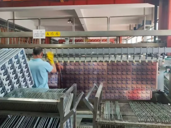
production workshop at Jerico.
A 4-layer or 6-layer PCB decision is fundamentally a stack-up decision — not merely a layer-count decision.
Quick Takeaway
Choose a 4-layer FR-4 board when your design can be routed within two signal layers, with finished holes ≥0.2 mm and you can accept lead-free HASL surface finish. Choose a 6-layer FR-4 board when high routing density pushes traces down to 3 mil, stable reference planes are required for impedance control and EMC performance, or fine-pitch components demand a flat ENIG surface. Copper weight is an independent critical factor: for high-current applications, a 2 oz copper construction such as PCB-54 often changes the design outcome more than adding two extra PCB layers.
This comparison references three standard specifications from SHENZHEN JERICO MULTILAYER PCB CO., LTD (Jerico). Founded in 2009, Jerico manufactures rigid PCBs from 1 to 18 layers and offers partial PCB assembly. Its 20,000 m² factory has a monthly capacity of 50,000–70,000 sqm. All content below is based solely on the published specs of PCB-10, PCB-55, PCB-54 and Jerico’s documented production capabilities. No estimated pricing, yield or performance data is included.
1. Why Layer Count Alone Cannot Guide Your PCB Selection
Many RFQs come with a fixed layer count, simply because an older product used 4 layers, or buyers assume 6-layer boards are inherently more reliable. Neither is a valid technical specification. Layer count only tells the fabricator how many copper layers to laminate. It does not tell you whether your traces can be routed successfully, whether impedance targets are achievable, or whether the surface finish suits fine-pitch components.
A proper evaluation sequence should answer these questions first:
- How many signal layers does your netlist actually require?
- What is the minimum finished hole size?
- What is the smallest line width and spacing?
- How much current flows through power traces?
- What surface flatness does your SMT assembly process require?
Each question corresponds to a stack-up parameter, covered in our three reference board specs.
- Forcing a design into 4 layers when 6 layers are needed leads to overly narrow traces and insufficient plane layers, which triggers manufacturability issues only after quotation.
- Specifying 6 layers unnecessarily adds extra inner-layer tooling, longer lamination cycles and approval lead time without gaining routing benefits.
In standard FR-4 stack-up practice:
- 4-layer PCB: typically 2 signal layers + 2 plane layers
- 6-layer PCB: typically 4 signal layers + 2 plane layers This structural difference drives most routing, EMC and sourcing trade-offs for consumer and industrial control boards.
2. The Multilayer FR-4 PCB Market Context
Multilayer PCBs remain the backbone of the global PCB industry. According to the 2026 Business Research Insights report, multilayer PCBs account for around 52% of worldwide PCB output volume. Prismark forecasts the global bare PCB market to reach approximately USD 95.8 billion in 2026, up from USD 85.8 billion in 2025, with China contributing roughly 60% of global PCB production capacity.
For buyers, this means 4-layer and 6-layer FR-4 capacity is widely available across China and is no longer a differentiator between suppliers. What separates qualified manufacturers is their capability envelope: minimum drill size, minimum line & space, impedance tolerance, surface finish options, plus full certification and documentation support. That is where your 4-layer / 6-layer selection becomes a strategic sourcing decision, not just a technical check.

3. Breakdown of Our Three Reference PCB Specifications
The three Jerico reference boards are built for different core requirements: layer count, copper weight, finished thickness, minimum feature size and surface finish.
3.1 PCB-10: The Cost-Effective 4-Layer Standard Board
PCB-10 is a 4-layer FR-4 PCB with 1 oz copper. Available finished thickness: 1.0 mm / 1.2 mm / 1.6 mm. Minimum finished hole: 0.2 mm. Surface finish: lead-free HASL. Compliance: UL, TS16949, RoHS, REACH, CQC.
- 1.0 mm / 1.2 mm options suit slim consumer enclosures and low-profile modules.
- 1.6 mm is selected when the PCB acts as a structural carrier, supports through-hole connectors or withstands repeated plugging.
- 0.2 mm minimum hole defines its standard via limit; smaller vias require HDI technology instead of standard 4-layer processing.
- 1 oz copper works for general signal routing and low-current power distribution.
- Lead-free HASL is RoHS-compliant and low-cost, but limited by uneven surface flatness — not ideal for fine-pitch and bottom-terminated components.
3.2 PCB-55: The High-Density 6-Layer Upgrade
PCB-55 is a 6-layer PCB, 1.6 mm thickness, 1 oz copper, 3 mil minimum line & space, ENIG finish. Two key upgrades come with the extra layers:
- More routing channels and dedicated reference planes
- 3 mil fine-line capability to fit more traces within the same board footprint
ENIG provides a flat, oxidation-resistant pad surface, which is critical for reliable soldering of fine-pitch and bottom-terminated components. Most industrial control designs move from 4-layer to 6-layer not for “higher robustness”, but because routing density cannot fit comfortably within a 4-layer stack-up.
3.3 PCB-54: High-Current 2 oz Copper Board with ENIG
PCB-54 features 2 oz copper, ENIG surface finish and blue solder mask. Its core value is higher current carrying capacity and improved thermal dissipation, rather than layer count. 2 oz copper conductors handle motor, relay, LED and power supply currents far better than standard 1 oz copper.
Blue solder mask is not purely aesthetic. Per Jerico’s finish guideline, blue solder mask delivers stable, medium dielectric constant and is recommended for high-speed impedance-controlled boards. Black solder mask has a higher dielectric constant and requires impedance simulation before production. If you select mask color only for appearance, always confirm its impact on impedance performance.
4. How to Resolve Mixed Requirement Scenarios
Design constraints often overlap, and you need to prioritize requirements:
- If you need 6-layer routing density plus local high-current paths: use PCB-55 as base stack-up, and confirm localized heavy copper with the manufacturer, instead of upgrading the whole board to 2 oz.
- If you need thin board thickness with only low current: PCB-10 (1.0 mm /1.2 mm) is the simpler, lower-cost option. Always follow specification constraints, not layer count.
5. Step-by-Step Selection Framework
- Count required signal layers from your netlist, not old habits. 2 signal layers + 2 planes → PCB-10. 4 signal layers or multiple power planes → PCB-55.
- Check minimum finished hole. ≥0.2 mm stays within standard 4-layer process; smaller holes belong to HDI.
- Check minimum line and space. Designs above 3 mil are mainly limited by surface finish; designs approaching 3 mil use PCB-55.
- Calculate trace current. 1 oz copper fits logic and low-current power; use 2 oz copper (PCB-54) for load-carrying traces to reduce voltage drop and improve thermal performance.
- Select surface finish based on component pitch, not only cost. Lead-free HASL for conventional pitch; ENIG for superior flatness, oxidation resistance and long shelf life.
- Set board thickness by mechanical requirements. 1.0 /1.2 mm for compact consumer housings; 1.6 mm for connector retention, card-edge and industrial mounting.
- Lock compliance documents before release. PCB-10 supports UL, TS16949, RoHS, REACH, CQC. Jerico factory holds ISO 9001, ISO 14001, IATF 16949:2016 (Cert. NQA:T184224, IATF:0493049, IATF USI:6GXSFM, valid 2023-12-22 ~ 2026-12-21), UL File No.E519316, CQC. RoHS, REACH and SGS reports available upon request.
- Confirm stack-up customization scope. Jerico supports full custom PCB fabrication from prototype to mass production: adjustable layer count, board thickness, inner/outer copper weight, plated copper, base material & Tg, blind/buried/resin-filled vias, via-in-pad, controlled impedance (±10% tolerance), PTH/NPTH, surface treatment, solder mask / silkscreen color, panelization and outline tolerance.
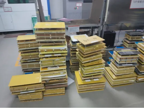
Electrical test, flying probe and fixture testing are the last verification point before shipment on either stack-up
6. Application Match: Consumer Electronics vs Industrial Control
6.1 Consumer Electronics
Consumer PCBs prioritize slim profile, cost and assembly speed over extreme routing density. PCB-10 (1.0 /1.2 mm, 1 oz, lead-free HASL) is widely used for smart home controllers, adapters, chargers, small home appliances and 3C accessories. Key limitation: once fine-pitch or bottom-terminated ICs are used, surface finish, not layer count, becomes your bottleneck.
6.2 Industrial Control
PLC I/O modules, sensor interfaces, motor drives and instrumentation typically require the stable reference planes and extra routing space of 6-layer boards. These products commonly adopt fine-pitch components that benefit from ENIG. PCB-55 (1.6 mm, 3 mil line/space, ENIG) is the baseline reference. For industrial products with long service life, full documentation and traceability are equally important as PCB performance, so define incoming inspection rules before placing mass orders.
High-Power Boards & LED Drivers
When PCB traces act as main power conductors, PCB-54 (2 oz copper + ENIG) is the suitable spec. Jerico shared customer project references:
- Brazil EMS: LED driver PCBs, 300K pcs over 6 years, defect rate 0.3%–0.8%, 10% cost saving, +1 year product lifespan.
- India EMS/ODM: Payment device PCBs, 300K pcs, lead time shortened by 12 days.
- Russian end-user: Civil drone PCBs, 50K pcs over 8 years, sample lead time 3 working days. These are case-specific customer results and not universal performance guarantees.
Specification Comparison Table
| Specification | PCB-10 | PCB-55 | PCB-54 |
|---|---|---|---|
| Layer count | 4 | 6 | Customizable |
| Copper weight | 1 oz | 1 oz | 2 oz |
| Finished thickness | 1.0 / 1.2 / 1.6 mm | 1.6 mm | Customizable |
| Min line & space | Standard | 3 mil | Customizable |
| Min finished hole | 0.2 mm | Standard | Customizable |
| Surface finish | Lead-free HASL | ENIG | ENIG |
| Solder mask | Standard | Standard | Blue |
| Compliance | UL / TS16949 / RoHS / REACH / CQC | As agreed | As agreed |
Note: A dash / “Customizable” means the parameter is not fixed in this reference part. Confirm all specs with Jerico for your specific order. These three boards are not ranked against each other: PCB-10 solves thickness & cost; PCB-55 solves routing density; PCB-54 solves high-current demand. If your design needs all three features, a customized stack-up will be required.
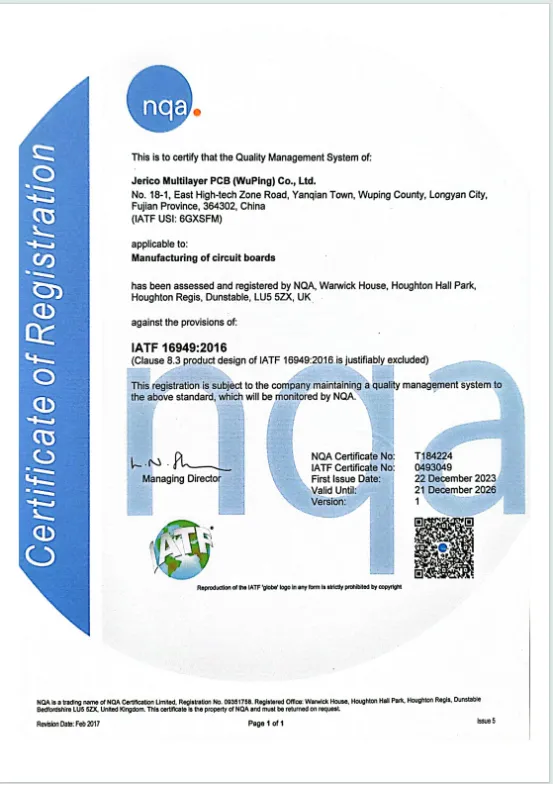
Factory-level IATF 16949:2016 certification supports industrial and automotive-adjacent control board programmes.
7. FAQ
7.1 What certifications and acceptance standards can we specify?
PCB-10 supports UL, TS16949, RoHS, REACH, CQC. Factory certifications: ISO9001, ISO14001, IATF16949:2016, UL E519316, CQC. Production follows IPC-A-600H, IPC-6012, UL-796. Acceptance criteria shall be written into purchase contracts. Pre-shipment test is standard; third-party SGS inspection is optional.
7.2 What stack-up capabilities should a Chinese multilayer PCB supplier provide?
Your supplier should support the full cycle from prototype to mass production within a stable process window, with customizable stack-up parameters. Jerico’s rigid multilayer process minimum line & space: 3 / 2.8 mil, controlled impedance tolerance ±10%.
7.3 What drives the cost difference between these three boards?
Cost is determined by process complexity rather than layer count alone.
- 2 oz copper: thicker plating and tighter etching control
- ENIG: extra nickel-gold chemical process vs HASL
- 3 mil fine features: higher imaging and inspection requirements
- Multiple thickness options: separate lamination setups
Jerico commercial terms: MOQ 1 pc, EXW, payment 30/70 or 50/50, lead time 7–45 days. Always quote based on your full stack-up instead of layer count only.
8. Can we validate stack-up with samples before mass production?
Yes. MOQ starts at 1 pc. Gerber, Protel 99SE, DXP, PADS9.5, AutoCAD, CAM350 files are accepted. Design data is strictly confidential; NDA available on request, files can be deleted after project completion per agreement. When requesting samples, provide layer count, thickness, copper weight, surface finish, solder mask / silkscreen color, quantity and reliability requirements.
9. What is the production lead time after stack-up approval? How to start?
Lead time ranges from 7 days (quick-turn prototype) to 45 days (mass production). Technical inquiries: reply within 24 hours. CAPA report available within 72 hours for quality issues. Send Gerber, stack-up details and quantity for quotation.
10. Conclusion
Choosing between 4-layer and 6-layer FR-4 PCBs hinges on five core variables: layer count, copper weight, board thickness, minimum feature size and surface finish.
- PCB-10 delivers cost-efficient 4-layer construction with flexible thickness options, 0.2 mm drill, lead-free HASL and full compliance.
- PCB-55 is the 6-layer high-density option with 3 mil fine lines and ENIG.
- PCB-54 addresses high-current needs with 2 oz copper, ENIG and stable blue solder mask.
If you specify based on these five parameters, your PCB matches your design. If you only specify by layer count, you either run out of routing space or pay unnecessary extra cost. The specification, not the layer count, is the real decision.
11. Next Step: Request Sample or Quotation
Share your Gerber files and target stack-up: layer count, finished thickness, copper weight, surface finish, solder mask color and quantity. Jerico will review manufacturability and send formal quotation. Prototype order: MOQ 1 pc, same process for mass ramp-up.
Email: sales@pcbjust.com
Tel / WhatsApp: +86 136-2097-2299
Website: https://www.pcbjust.com
Company profile: https://cdn.socialarks.com/sbsp/25249/common/2026/0827/JERICO PCB-company profile.pdf
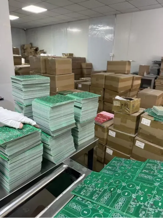
Finished boards move from final inspection to packing and shipment; documentation is issued per order