Realize your idea with PCB design.
Printed Circuit Board (PCB) Design refers to the engineered process of transforming electrical connectivity between electronic components into a physical layout. Using specialized software tools, it involves planning conductive pathways, component placement, and stackup structures on insulating substrates—while optimizing metal traces/vias, electromagnetic protection, thermal dissipation, and other critical factors—to ultimately generate standardized manufacturing files.
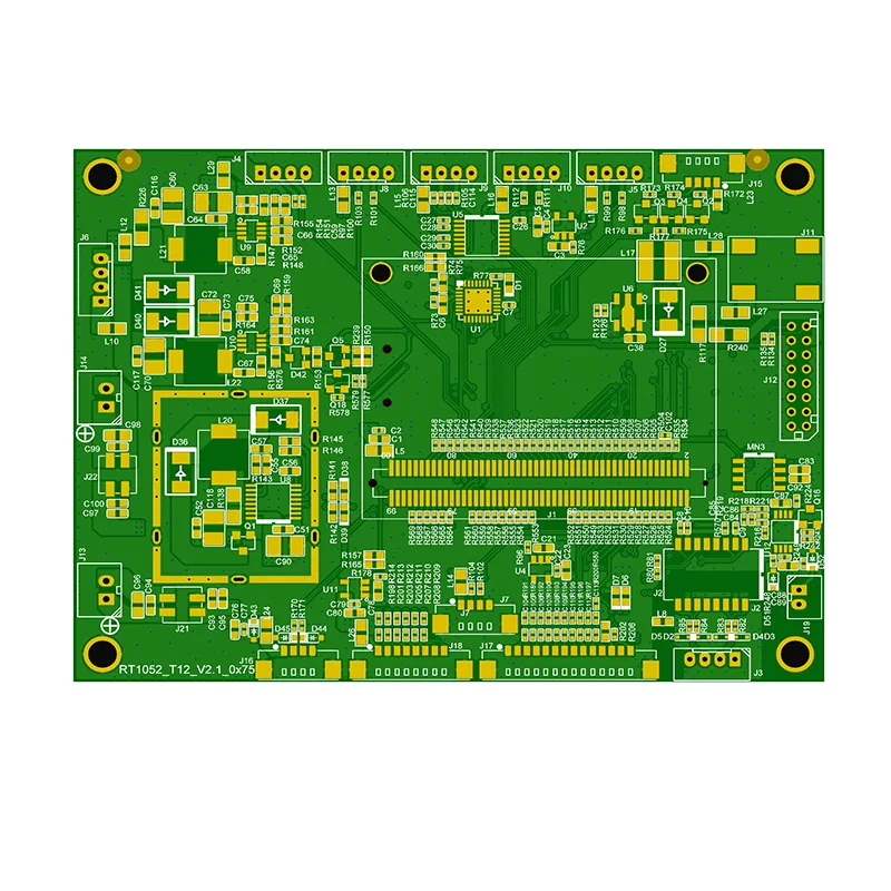
Superior PCB design reduces production costs while achieving optimal circuit performance and thermal management. And talking with Jerico team about your PCB design plan, is the right choice you made.
PCB Design Process:
What are the main stages of the PCB design workflow?
Stage 1: Customer Requirement Analysis and Schematic Design
- Clarify the customer’s product functional requirements, electrical performance specifications, and mechanical constraints. Select a suitable substrate material (e.g., FR-4 or high-frequency materials).
- Determine the circuit topology, plan functional module partitioning (e.g., power supply, signal processing, interfaces), and make an initial layer stackup decision (single-layer, double-layer, or multi-layer).
Stage 2: Schematic Design and Verification
- Use EDA tools (e.g., Altium Designer, KiCad) to draw the schematic, defining component connectivity and ensuring symbol-to-footprint matching.
- Verify for issues like shorts and opens using Electrical Rule Checking (ERC). Generate the netlist for subsequent layout stages.
Stage 3: Layout Planning
- Functional Partitioning: Divide areas based on signal types (high-frequency/sensitive/power), prioritizing placement of core components (e.g., MCU, power modules).
- Signal Flow Optimization: Arrange components along the input → processing → output path to minimize trace meandering. Keep high-frequency signal paths short and direct.
- Thermal and Mechanical Considerations: Reserve space for mounting holes and thermal vias. Ensure component spacing complies with mechanical structure requirements.
Stage 4: Routing and Impedance Control
- Priority Routing: Route critical signals first (e.g., high-speed signals like clock lines, differential pairs), ensuring length matching and impedance matching.
- Power and Ground Plane Design: Widen power/ground traces; use copper pours to reduce impedance. Connect analog and digital grounds at a single point using magnetic beads or 0Ω resistors.
- Crosstalk Avoidance: Maintain sufficient spacing (≥ 3x trace width) between sensitive signals and high-current traces. Use orthogonal routing directions between adjacent layers.
Stage 5: Design Rule Check (DRC) and Simulation Verification
- Check trace width/spacing, via sizes, etc., for compliance with manufacturing specifications.
- Perform signal integrity simulations (e.g., rise time, ringing, impedance continuity) to ensure performance targets are met.
- Prepare and output production files.
Stage 6: Production File Generation
- Generate Gerber files (for each copper layer, solder mask, silkscreen, etc.), NC Drill files, and the Bill of Materials (BOM) for factory fabrication.
Share your ideas with the Jerico design team—we’ll realize your idea for sure.